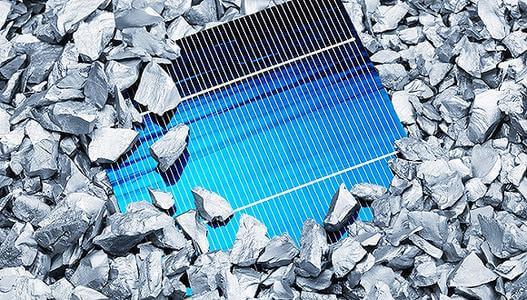
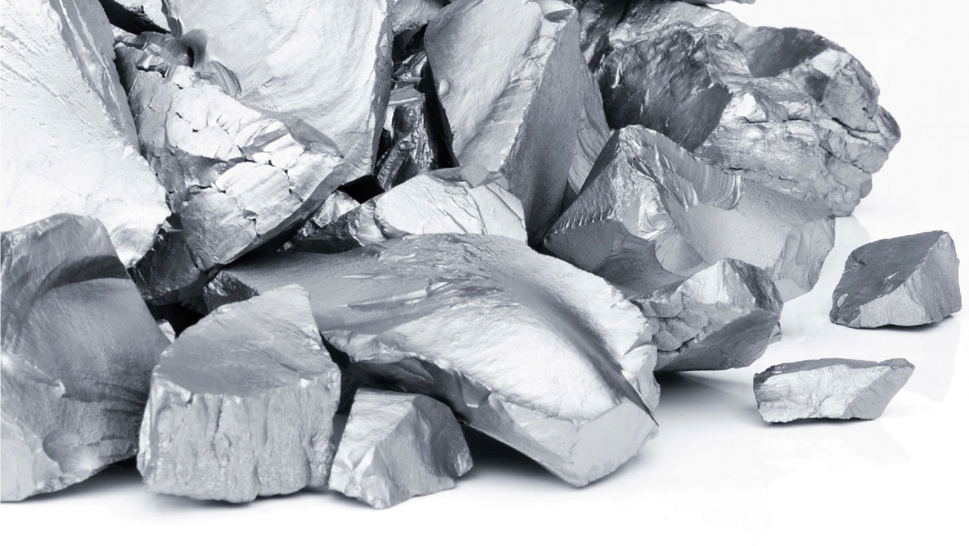
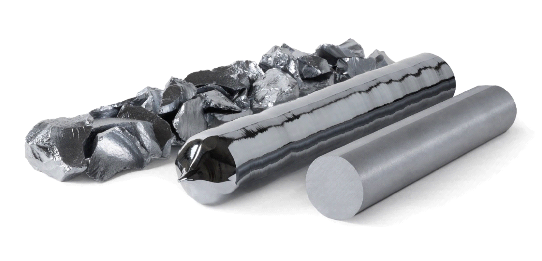
Plant & Tech Poly Silicon

Poly Silicon

Comparison of purity of different grades of silicon

Silicon, which is considered as the second most abundant substance in the earth’s crust, is found as the silica (SiO2) compound is extracted from stones rich in silica with an appropriate purity. These stones come with large amounts of impurities in nature which the first stage is dedicated to reduction of impurities and purifying silica to obtain silicon with metallurgical grade with a purity more than 98 percent silicon. In the following section, we will deal with the production process of this purification until making polysilicon with solar grade and/or semi-conductor grade. The purity of silicon required for being used in solar panels is 99.9999 percent which is called 6N. Also, the purity required for producing semi-conductors varies from 9N to 11N. In the following table, quantity of each impurity existing in silicon in three different grades has been shown

To purify silicon, various methods are used. These methods are divided into two categories in general:
⦁ Metallurgical methods
⦁ Chemical methods

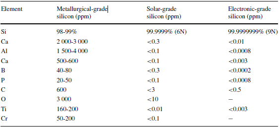
First method cannot take the separation process to the intended amount in terms of omitting the impurities related to phosphorus and boron but if some process corrections are made, we can expect 6N purity. Metallurgical methods are consisted of a number of melting and freezing stage operations and no chemical substance is used.
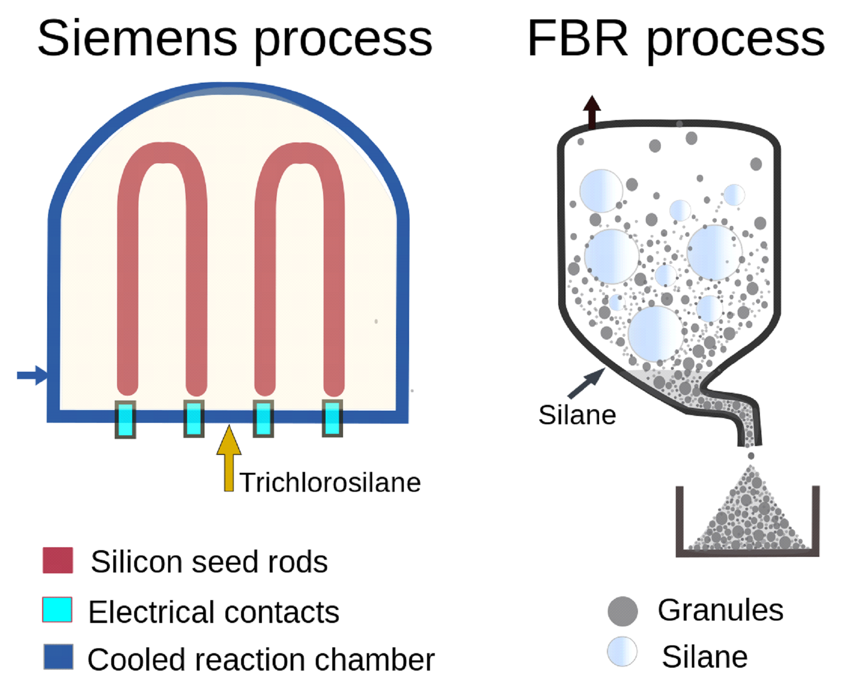
Second method, which reaches the intended purity through chemical reactions and numerous separating processes, performs much more successfully in omitting impurities in particular impurities related to boron and phosphorus. In chemical methods, pure silicon is obtained through chemical reactions and they can be divided into two categories:
⦁ Hydrogen decomposition or reduction of silane compounds
⦁ Hydrogen decomposition or reduction of silicon tetrahalides

First category methods create different silane compounds using different and consecutive reactions. Given the number of chlorine and hydrogen existing in their structures, the following five compounds can be used for producing pure silicon as well:
⦁ Monosilane (SiH4)
⦁ Chlorosilane (SiH3Cl)
⦁ Dichlorosilane (SiH2Cl2)
⦁ Trichlorosilane (SiHCl3)
⦁ Tetrachlorosillane or silicon tetrachloride (SiCl4)

Silicon tetrachloride can be examined in tetrahalides category. Two common compounds for producing pure silicon are monosilane (or silane in short) and trichlorosilane. Other compounds are rarely used as raw material of decomposition reactor. Silane (SiH4) and trichlorosilane (SiG3Cl) can convert into silicon alone or in the presence of hydrogen. Usually, monosilane is decomposed, whereas trichlorosilane is reduced with help of hydrogen. Also, these two compounds enter into a fluidized bed reactor and produce granular silicon or enter into a reactor with U-shaped silicon rods and deposit on the surface of rods on which we will talk in the following sections. In fact, in both states, silicon cores already exist and their sizes increase with the progress of decomposition reaction. In first state, silicon cores are present in the form of very small spherical seeds and the second mood, silicon cores are present in the form of thin rods. Given the above moods as well as conditions of temperature and pressure, different companies use various technologies. But, in general, these technologies are either based on trichlorosaline or monosaline. The most famous method based on trichlorosaline is the process of Siemens Company and the most famous method based on monosaline is the process of Union Carbide Company. It should be mentioned that share of Siemens technology in solar silicon production industry is much more than that of other existing technologies. In second category of chemical reactions, decomposition or reduction of tetra iodide, tetra bromide and tetra sodium chloride or other silicon halogen compounds are used.

Poly Silicon Stats

+0

Manpower absorbed

0

Manpower development

+0M$

Investment

+0%

Progress

First, growth of silicon crystals was realized with Float Zone method and then, some methods were founded which fulfilled the goal to produce large, flat and even silicon surfaces with at a low cost. Gradually, these methods increased the diameter of wafer from around 0.5 mm to 300 mm commercially. In research, increase of wafer diameter up to more than 450 mm has been reported and is followed up by different research groups as a very important issue. In general, similar technology of crystal growth and sublayer is being evolved significantly to meet the ever-increasing needs of solar industry by providing unique manufacturing platforms. Different subsets of industrial production of polysilicon based on Siemens method and silicon wafer are shown in the following figure as two final products of Azar Silicon Co.

Based on project progress according to design and feasibility study conducted, Azar Polysilicon Factory is at the stage of completing the investors loop. After determining the combination of investors, procurement and execution operation of Azar Polysilicon Factory will be commenced by choosing the best geographical location from among locations examined.